


5 PCB Stencil Design Rules to Avoid Solder Bridges and Beads at the Source 🛠️
 View
View
If your SMT assembly is plagued by solder bridges, mid-chip beads, or inconsistent deposits, the fix isn't just in your soldering iron - it's in the physics of your SMD stencil.
To achieve professional-grade results and prevent reflow defects, we explored 5 tips for your PCB Stencil design:
1. Aperture Design Guidelines
To prevent solder flaws like bridging and solder beads, this is crucial. For accurate deposition the apertures are made to be a bit smaller than the pads. However, for certain parts, an aperture with a specific design is required to deposit less paste on the inner edge of the part, which helps to prevent the formation of "mid-chip" solder balls. Here are a few instances:
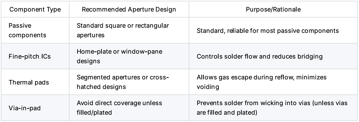
Aperture Reduction (Pad-to-Aperture Ratio)
Apertures are frequently made slightly smaller than the actual pad dimensions in order to prevent bridging and extra solder. Here is a table of selection:
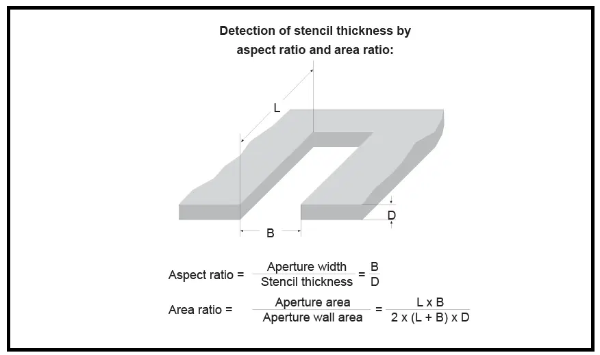
Recommended Thickness Rules:
For most components, the typical reduction is between 5 and 7%.
For dependable printability, IPC-7525 suggests a stencil-to-pad area ratio >0.66.
Formula:
Area Ratio = (Aperture Area) / (Aperture Wall Height × Aperture Perimeter)
Keep this ratio above 0.66 to ensure clean paste release.
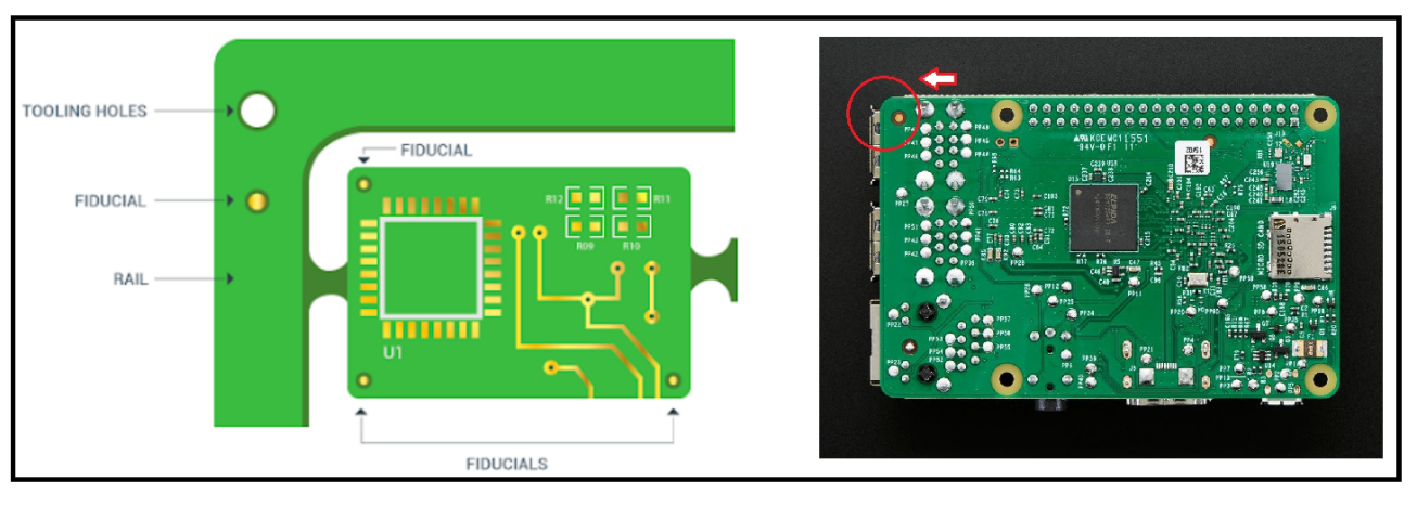
Fiducial Marks
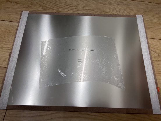
When printing solder paste onto pads, it is very important that the pattern is lined up correctly with the PCB. This is accomplished by applying fiducial marks, which are registration marks, to the PCB and stencil. As you can see from our most recent comprehensive piece on fiducial marks, adding them to the stencil will guarantee proper alignment. JLCPCB provides stencils with fiducial marks included, helping ensure accurate alignment and reliable solder paste printing.
Stencil Frame and Border
Stencils can be frameless (for rapid prototyping or manual printing) or framed (glued into aluminum frames).
Typical frame dimensions are 23 x 23 inches.
Keep the distance between the aperture area and the frame edge at least 10 mm.
Mark the stencil's position, thickness, and part number clearly.
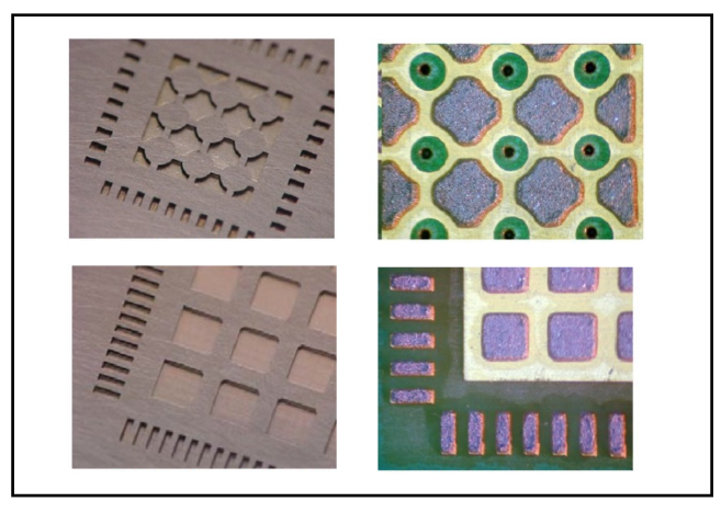
Window Effect design
There are instances where the PCB design features big copper pads underneath the component. Devices that use power electronics typically experience this. In this case, a window effect is present to ensure a good electrical link and to let the device's heat escape. The device may lift and the outer leads may not solder if solder paste is placed over the entire pad. A "window effect" in the design can be used to decrease the solder volume, which is shared in the image above.
🚀 Turn Your Designs into Reality with JLCPCB
Whether it's a standard build or a complex custom project, we support your unique designs with high-precision stencils to make your SMT assembly faster, smoother, and more reliable.
- 🎁 Claim your $10 Stencil Coupon, and get your customized PCB Stencils here!
- ✨ New User Bonus: Register for a $123 Coupon Bundle!
Sign In Or Register Comment after
No comments yet. Be the first to comment!